Différences entre les versions de « Zone of characterisation »
(ajout du lien vers la page cible à partir du drapeau) |
(correction de l'anglais) |
||
| Ligne 15 : | Ligne 15 : | ||
==Organic Field Effect Transistors (OFETs)== | ==Organic Field Effect Transistors (OFETs)== | ||
| − | <p>The measurement of | + | <p>The measurement of output and transfert caracteristics of organic field effect transistors is carried out under inert atmosphere. Several configurations are available (Fig. 1):</p> |
<ul><li>bottom contact/top gate (a)</li> | <ul><li>bottom contact/top gate (a)</li> | ||
<li>bottom contact/bottom gate (b)</li> | <li>bottom contact/bottom gate (b)</li> | ||
| Ligne 22 : | Ligne 22 : | ||
Fig. 1: Different configurations available for the OFETs</center></p> | Fig. 1: Different configurations available for the OFETs</center></p> | ||
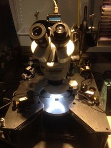
| − | <p>The dimensions of the channel of the transistor are variable and depend on the chosen configuration. The channel is made either of a single compound (electron donor or acceptor) of the active layer of a photovoltaic cell (Fig. 2), or of a blend of electron donor and acceptor. Transfer characteristics are measured with a Keithley 4200 SCS system (Fig. 3). They allow the estimation of the mobility of | + | <p>The dimensions of the channel of the transistor are variable and depend on the chosen configuration. The channel is made either of a single compound (electron donor or acceptor) of the active layer of a photovoltaic cell (Fig. 2), or of a blend of electron donor and acceptor. Transfer characteristics are measured with a Keithley 4200 SCS system (Fig. 3). They allow the estimation of the mobility of charge carriers by using the usual OFET's formalism.</p> |
<table border="0" cellpadding="5" cellspacing="1" style="width:100%;"> | <table border="0" cellpadding="5" cellspacing="1" style="width:100%;"> | ||
| Ligne 30 : | Ligne 30 : | ||
<td>Fig. 3: Output characteristics of an OFET: I<sub>ds</sub> is the drain-source current, V<sub>ds</sub> the drain-source voltage and V<sub>g</sub> the gate voltage.</td></tr></table> | <td>Fig. 3: Output characteristics of an OFET: I<sub>ds</sub> is the drain-source current, V<sub>ds</sub> the drain-source voltage and V<sub>g</sub> the gate voltage.</td></tr></table> | ||
<br/> | <br/> | ||
| − | <p>OFETs have various applications, | + | <p>OFETs have various applications, and [[Chemical sensors|chemical sensors]] are one of them.</p> |
<br/><br/> | <br/><br/> | ||
==Space Charge Limited Current (SCLC) devices== | ==Space Charge Limited Current (SCLC) devices== | ||
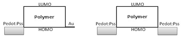
| − | <p>The measurement of | + | <p>The measurement of I(V) characteristics of a diode with a single type of carriers allows the estimation of the mobility of charge carriers if the current is limited by the space charge. Thus, a SCLC device is a semiconducting layer sandwiched between two electrodes whose extracting work is chosen to inject only electrons or only holes. The choice of these electrodes depends on the boundary energy levels of the organic semiconductor under study (Fig. 4). Devices of several thicknesses are necessary to ensure that the current is effectively limited by the space charge and not by carrier injection (same dependence: I proportional to V<sup>2</sup> in in both cases). I(V) measurements (Fig. 5) are done under controlled atmosphere and the thickness of the active layer is ascertained by profilometry.</p> |
<table border="0" cellpadding="5" cellspacing="1" style="width:100%;"> | <table border="0" cellpadding="5" cellspacing="1" style="width:100%;"> | ||
Version du 12 janvier 2017 à 15:25
 |
 |
 |
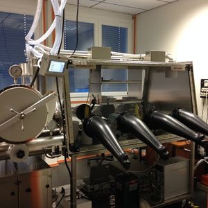
Contact: Sadiara FALL
This equipment has been funded by ICube and IPCMS ("Institut de Physique et Chimie des Matériaux de Strasbourg").
Organic Field Effect Transistors (OFETs)
The measurement of output and transfert caracteristics of organic field effect transistors is carried out under inert atmosphere. Several configurations are available (Fig. 1):
- bottom contact/top gate (a)
- bottom contact/bottom gate (b)
- top contact/bottom gate (c)
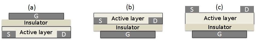
Fig. 1: Different configurations available for the OFETs
The dimensions of the channel of the transistor are variable and depend on the chosen configuration. The channel is made either of a single compound (electron donor or acceptor) of the active layer of a photovoltaic cell (Fig. 2), or of a blend of electron donor and acceptor. Transfer characteristics are measured with a Keithley 4200 SCS system (Fig. 3). They allow the estimation of the mobility of charge carriers by using the usual OFET's formalism.
 |
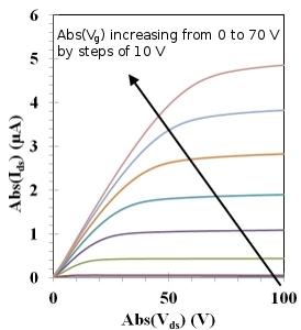 |
| Fig. 2: Channel of an OFET in configuration bottom contact/bottom gate viewed with an optical microscope. This channel is made of a small semiconducting molecule. | Fig. 3: Output characteristics of an OFET: Ids is the drain-source current, Vds the drain-source voltage and Vg the gate voltage. |
OFETs have various applications, and chemical sensors are one of them.
Space Charge Limited Current (SCLC) devices
The measurement of I(V) characteristics of a diode with a single type of carriers allows the estimation of the mobility of charge carriers if the current is limited by the space charge. Thus, a SCLC device is a semiconducting layer sandwiched between two electrodes whose extracting work is chosen to inject only electrons or only holes. The choice of these electrodes depends on the boundary energy levels of the organic semiconductor under study (Fig. 4). Devices of several thicknesses are necessary to ensure that the current is effectively limited by the space charge and not by carrier injection (same dependence: I proportional to V2 in in both cases). I(V) measurements (Fig. 5) are done under controlled atmosphere and the thickness of the active layer is ascertained by profilometry.
 |
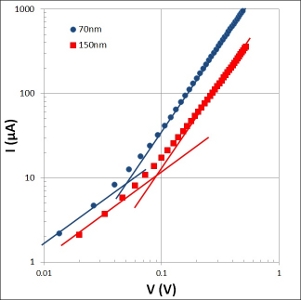 |
| Fig. 4: SCLC devices for the measurement of hole mobility. HOMO (Highest Occupied Molecular Orbital) and LUMO (Lowest Unoccupied Molecular Orbital) are the boundary orbitals of the small molecule or of the semiconducting polymer. | Fig. 5: I(V) curves measured for SCLC devices whose active layer (two different thicknesses) is made of a small semiconducting molecule. The ohmic regime (I proportional to V) is observed at low voltage and the SCLC regime (I proportional to V2) at voltages higher than 0.1 V. |